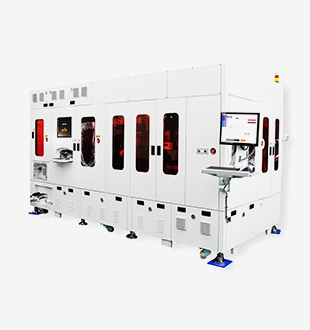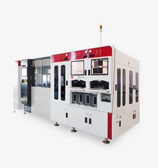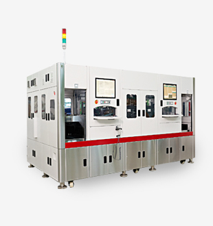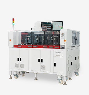
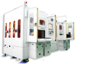

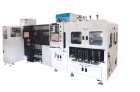
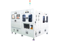
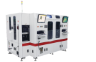
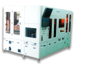

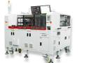
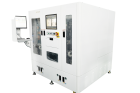
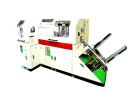


반도체 장비 제조 기술의 리더, 제너셈
Leader’s Choice
Genesem
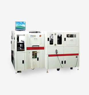
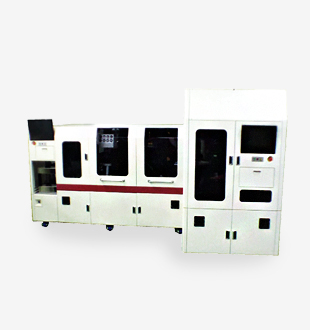
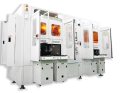
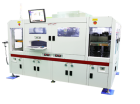
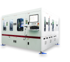
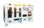
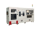
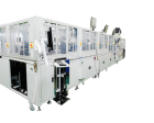
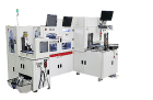
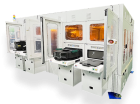
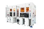
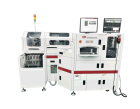
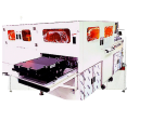
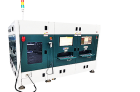
반도체 제조용 장비와 레이저를 이용한 반도체 완성품 패키지,
PCB 마킹 장비, 비전 검사장비 등을 보유하고 있으며, 국내를 비롯해
미국, 중국, 멕시코, 필리핀 등 세계 시장에 공급하고 있습니다.
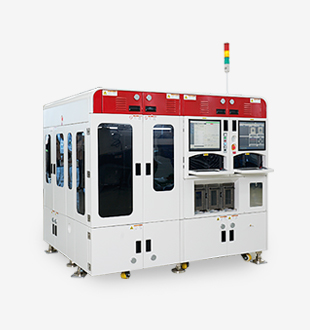
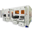
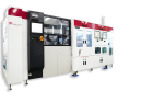
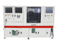
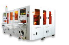
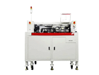
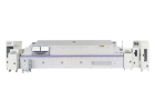
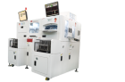
반도체 장비 제조 기술의 리더, 제너셈
Advanced
Technologies
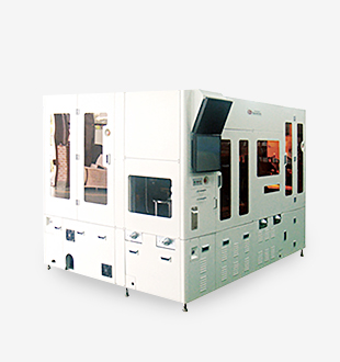
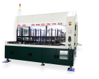
차별화된 설계 및 기술 경쟁력을 더욱 제고해 한 단계 높은 성장으로
기업가치를 극대화하고 명실상부한 글로벌 리더로 발돋움 하겠습니다.
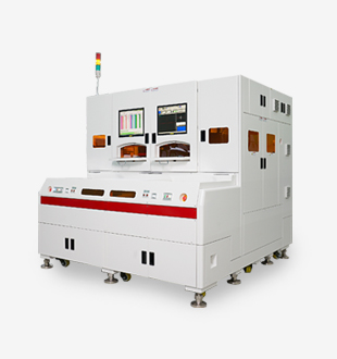
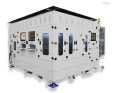
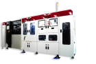
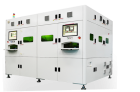
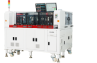
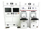
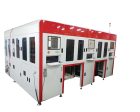
반도체 장비 제조 기술의 리더, 제너셈
Sustainable
Growth
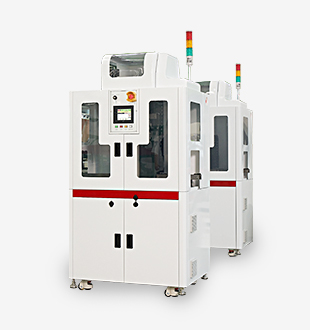
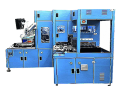
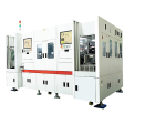
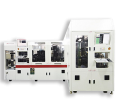
반도체 후공정 장비 제조 전문 기업, 제너셈은
독보적인 기술력과노하우로 국내 1위는 물론
세계적으로 인정받는 기업으로 성장하겠습니다.
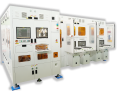
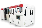
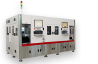
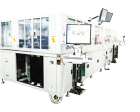
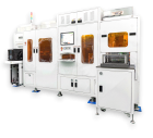
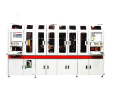
반도체 장비 제조 기술의 리더, 제너셈
Genesem
for Tomorrow
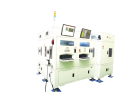
열정과 창의적인 인재가 제너셈의 미래를 이끕니다.
창의적이고 혁신적인 제너셈인들은 단단한 초석이 되어 대한민국
반도체장비 산업을 이끌어 갈 것입니다.